
Technology Fields
- GaAs Electronic Devices (HBT, pHEMT, etc.)
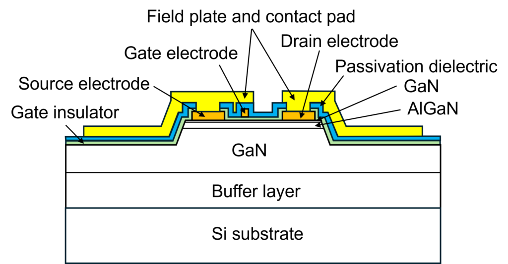
- GaN Electronic Devices (GaN HEMT, MISHEMT, Diodes, etc.)
- Large-Signal Device Modeling
Collaboration

Hosei University
GaN MISHEMT, GaN pn-Diode

Nagoya Institute of Technology
GaN/Si epitaxy, ALD GaN MISFETs

Hiroshima University
GaN/Si Power Devicess
サービス案内
GaN Power Device R&D
Collaboration with Hosei University and Nagoya Institute of Technology
Compound Semiconductor Device Consulting
Introduction of foundry service companies
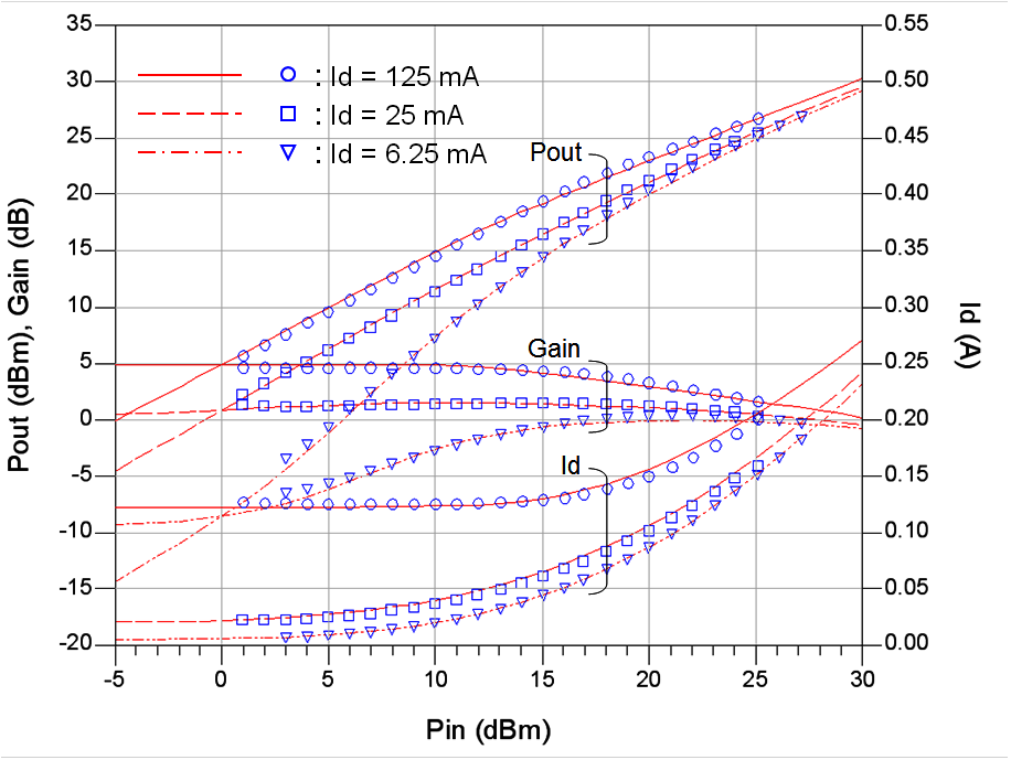
Large-Signal Device Modeing
GaN HEMT, GaAs pHEMT, etc.